LVDS PCB Layout – Expert Guidelines You Need to Know! Pcb layout design by siemens
We talkin' 'bout PCB design, right? It's like the backbone, the nervous system, the *soul* of any electronic device. You mess this up, and yo' whole project just gon' crash and burn. No bueno. So, pay attention, absorb this info, and level up your game.
Top PCB Design Guidelines Every Designer Needs to Know

First thing's first, we gotta talk about minimizing noise. Imagine tryin' to listen to your favorite track with a bunch of static and crackling. Annoyin', right? Same thing with electronics. Noise interferes with signals, causing malfunctions and errors. Key to squashing that noise? Proper grounding. Ground planes, star grounding – learn 'em, love 'em, live 'em. And keep those traces short and sweet, especially for high-speed signals. Longer traces act like antennas, pickin' up unwanted interference. Nobody got time for that.
Next up: signal integrity. This is all about making sure the signal you send is the signal you receive. No distortions, no reflections, no funny business. Things like impedance matching become super important here. Think of it like a pipe. If the pipe's width changes suddenly, the water flow gets disrupted. Same with signals. Keep that impedance consistent throughout the trace to avoid reflections that can mess up your data.
Power distribution. Gotta make sure everything's gettin' enough juice, but not too much, ya dig? Use wide traces or power planes to deliver current efficiently and minimize voltage drops. Decoupling capacitors are your friends. Place 'em close to the chips that need 'em to filter out noise and provide a stable power supply. Think of 'em like little emergency power stations right next to the users.
PTN3460 DP to LVDS PCB Layout Guidelines

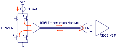
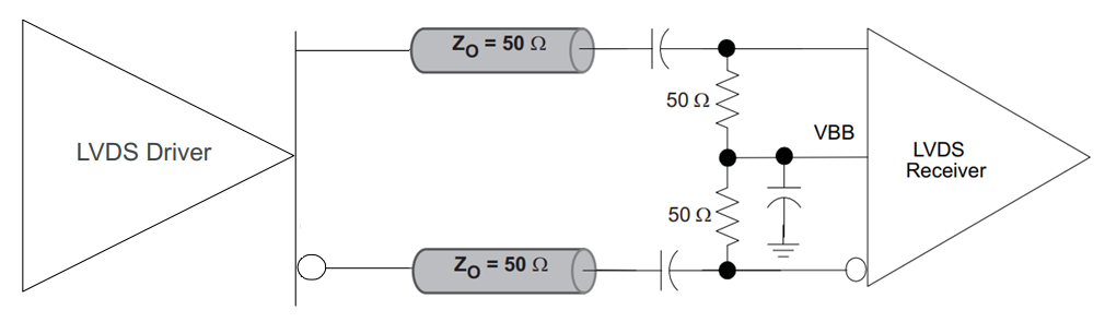
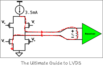
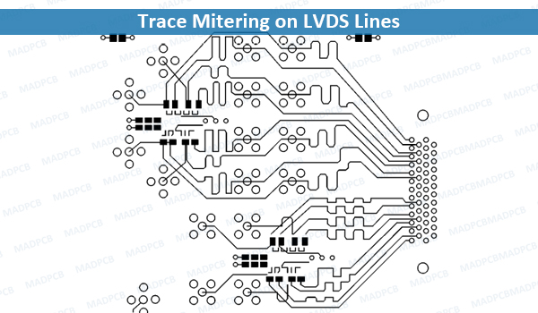
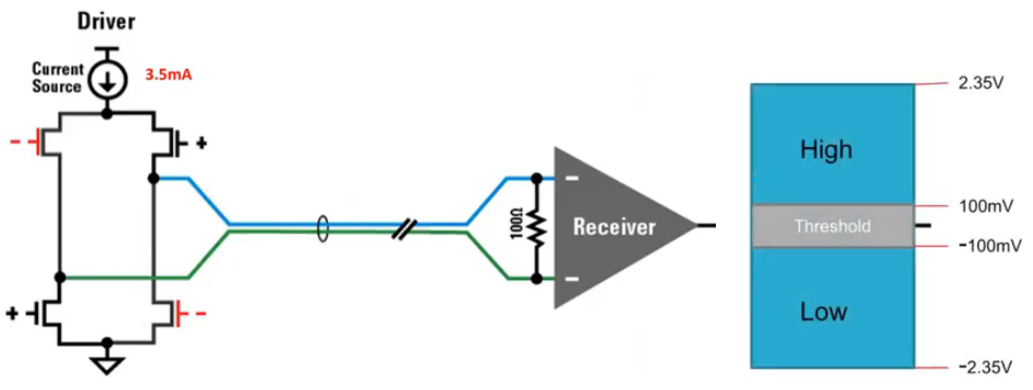
Now, let's get specific with DP (DisplayPort) to LVDS (Low-Voltage Differential Signaling). This is where things get a little more complex. DP is a high-speed digital interface, and LVDS is often used to drive displays. Getting these two to play nice requires careful layout. Pay close attention to the differential pairs. They gotta be routed together, side-by-side, with matched lengths. Any mismatch can cause timing skew and signal degradation. Keep 'em away from noise sources like power supplies and clock signals. Crosstalk is real, y'all.
Also, consider the impedance control. DP and LVDS have specific impedance requirements, usually around 100 ohms. Use a PCB design tool that allows you to calculate trace widths and spacing to achieve the desired impedance. And don't forget about termination. Proper termination at the receiver end is crucial to prevent reflections and ensure signal integrity. Resistors, y'all, resistors! Make sure you're using the correct values and placing them correctly.
Finally, remember that good PCB design is an iterative process. Don't be afraid to experiment, simulate, and test your designs. Use a good PCB design software package that allows you to analyze signal integrity and simulate circuit performance. And don't be afraid to ask for help. There are plenty of experienced PCB designers out there who are willing to share their knowledge. Keep learning, keep practicing, and you'll be buildin' circuits like a seasoned pro in no time!
If you are looking for Practical PCB design layout rules - Leading PCB Manufacturer - Arisentec® you've came to the right web. We have 25 Images about Practical PCB design layout rules - Leading PCB Manufacturer - Arisentec® like Some LVDS PCB Layout Guidelines For Ensuring Signal, 40% OFF, Some LVDS PCB Layout Guidelines For Ensuring Signal, 40% OFF and also (PDF) AN11088 PTN3460 DP to LVDS PCB layout guidelines - DOKUMEN.TIPS. Read more:
Practical PCB Design Layout Rules - Leading PCB Manufacturer - Arisentec®
 arisentecpcb.com
 Pcb Layout Guidelines For Design By PCBCART - Issuu
 issuu.com
 (PDF) AN11088 PTN3460 DP To LVDS PCB Layout Guidelines - DOKUMEN.TIPS
dokumen.tips Practical PCB Layout Tips Every Designer Needs To Know
 www.scribd.com
 Some LVDS PCB Layout Guidelines For Ensuring Signal, 40% OFF
 www.oceanproperty.co.th
 Some Lvds Pcb Layout Guidelines For Ensuring Signal I - Vrogue.co
 www.vrogue.co
 PCB Design Layout Guidelines For Engineers | Advanced PCB Design Blog
 resources.pcb.cadence.com
 Some LVDS PCB Layout Guidelines For Ensuring Signal Integrity | PCB
 resources.altium.com
 Top PCB Design Guidelines Every PCB Designer Needs To Know | Altium
www.pinterest.co.uk The 13 Most Used PCB Layout Design Tools
 southelectronicpcb.com
 PCB Layout Design By Siemens | PADS Professional | Cadlog
 www.cadlog.com
 pcb xpedition software mentor pads integrated environment siemens descrição detalhada
PCB Layout Rules For PCIE, SATA, LAN, LVDS, USB, SDVO,
 www.fedevel.com
 BASIC PCB Design Rules – Layout
 epci.eu
 Some LVDS PCB Layout Guidelines For Ensuring Signal, 40% OFF
 www.oceanproperty.co.th
 Top 5 PCB Design Rules You Need To Know | PCB Design Blog | Altium
 resources.altium.com
 PADS Standard Layout - Mentor Graphics
 www.pads.com
 pads layout pcb design reuse variants reduce errors assembly physical completion pdr accelerate learn mentor
Layout PCB Inverter: Tips And Best Practices For Successful Design
 hillmancurtis.com
 Some Lvds Pcb Layout Guidelines For Ensuring Signal I - Vrogue.co
 www.vrogue.co
 Some LVDS PCB Layout Guidelines For Ensuring Signal Integrity | PCB
PCB Layout Services – Electronics Engineering Design Services
 www.microelectronicos.net
 A Detailed Guide To PCB Layout Design - IBE Electronics
 www.pcbaaa.com
 Some LVDS PCB Layout Guidelines For Ensuring Signal, 40% OFF
 www.oceanproperty.co.th
 Some LVDS PCB Layout Guidelines For Ensuring Signal Integrity | PCB
 resources.altium.com
 PCB Layout Design By Siemens | PADS Professional | Cadlog
 www.cadlog.com
 pads pcb rf correct siemens
PCB Layout Design By Siemens | PADS Professional | Cadlog
 www.cadlog.com
 pcb routing flex rf nets rigid analog embedded constraint
Practical pcb layout tips every designer needs to know. Top 5 pcb design rules you need to know. Pcb layout services – electronics engineering design services